SPI-MEM-CTRL
Quad SPI Flash Memory Controller
|
|
|
|
The SPI-MEM-CTRL core from Alma Technologies is an advanced SPI serial NOR and serial NAND flash memory controller, supporting Single, Dual and Quad I/O SPI accesses and including Boot and Execute on-the-fly features.
The SPI-MEM-CTRL core is designed to provide to a host a simple interface for controlling SPI Serial Flash Memories. The core is highly flexible and can be configured before synthesis or programmed during runtime to support a large number of SPI Serial Flash memories, even less standard ones.
A host can interface to the Serial Flash in a number of ways. Transferring data from the Flash memory to the host is done with minimum effort with a Block Read Interface, which uses a DMA mechanism to transfer a block of data to the host’s memory space. Alternatively, the host can introduce a read request using the core’s programmable registers. Then the core serves this request and sends the necessary instructions to the Serial Flash device. An additional RAM like interface which permits on-the-fly code execution is also available.
The SPI-MEM-CTRL controller has been rigorously verified. A complete verification environment that helps designers verify the functionality and compliance of the core, including additional aids for system-level simulation, are available.

IP Deliverables
Clear-text RTL sources for ASIC designs, or pre-synthesized and verified Netlist for FPGA and SoC devices
Release Notes, Design Specification and Integration Manual documents
Bit Accurate Model (BAM) and test vector generation binaries, including sample scripts
Pre-compiled RTL simulation model and gate-level simulation netlist for the FPGA Netlist license
Self-checking testbench environment sources, including sample BAM generated test cases
Simulation and sample Synthesis (for ASICs) or Place & Route (for FPGAs) scripts
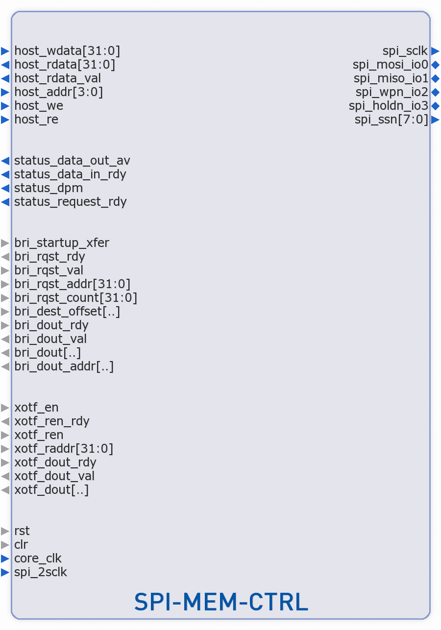
Symbol

Features
Device Independent:
Supports serial NOR and serial NAND SPI flash memories
Implements identification mechanism to detect connected serial flash memories
Configurable memory features to allow support for more serial flash devices
Efficient Bandwidth Utilization:
Automatic identification of maximum bandwidth access mode among:
single SPI
dual output SPI
dual I/O SPI
quad I/O SPI
Flexible Access Model:
Registered mapped I/O
NOR SPI Flash features:
Read access sizes from 1 byte up to memory density
Read accesses starting from any address offset
Write access sizes from 4 bytes up to memory density
Write accesses starting from any address offset that is 32-bit word aligned
Erasure of:
• any sector (4KB)
• any block (64KB)
• whole chip
NAND SPI Flash features:
Read access sizes from 1 byte up to memory density
Read accesses starting from any address offset that is 32-bit word aligned
Write access sizes from 4 bytes up to memory density
Write accesses starting from any address offset that is 32-bit word aligned
Erasure of:
• any block (128KB)
Ease of Integration:
Auto-detection of a wide set of serial flash devices to minimize programming overhead
Auto detection of the fastest way to read or program the memory, to maximize bandwidth and minimize programming overhead
Deep Power-down Mode support to minimize power consumption
Design Quality:
Robust verification with integrated self-checking testbench environment
Scan-ready design
